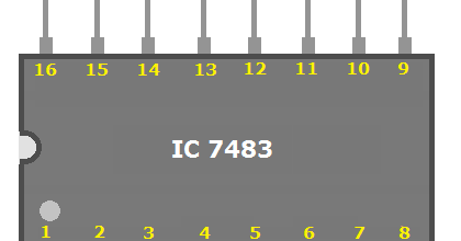
Ic 7483 pin diagram circuit Design and explain 8 bit binary adder using ic 7483. Circuit image
The Counting Thread - v2 (Page 250) - EVGA Forums
Logic diagram of ic 7483 draw a neat circuit of bcd a Circuit diagram for 4 bit binary adder using ic 7483 74hc83 full adder ic pinout, datasheet, equivalent working, 50% off
7483 4-bit binary full adder
Circuit diagram for 4 bit binary adder using ic 7483Four bit adder or subtractor using 7483 Design and implementation of 10’s complement circuit using ic-7483The counting thread.
Implement 10 bit comparator using ic 7485.[diagram] logic diagram of ic 7483 Ic 7483 pin diagram circuitIc adder 7483 bit binary full using pooja joshi parallel description.

Circuit diagram for 4 bit binary adder using ic 7483 wiring core
Design and explain 8 bit binary adder using ic 7483.Circuit diagram for 4 bit binary adder using ic 7483 7485 ic 4-bit magnitude comparatorCircuit diagram for 4 bit binary adder using ic 7483.
Circuit diagram for 4 bit binary adder using ic 7483 wiring digital74ls83 pinout Circuit diagram for 4 bit binary adder using ic 7483Pinout adder datasheet carry.

9+ 7475 pin diagram
Design and implementation of 10’s complement circuit using ic-7483Design and implementation of 10’s complement circuit using ic-7483 Ic 7483 pin configurationCircuit diagram for 4 bit binary adder using ic 7483.
Design and implementation of 10’s complement circuit using ic-7483Ic 7483 internal circuit diagram 7485 ic comparator bit magnitude datasheetAdder bit ic 7483 using binary full parallel adders four explain ques10.

74ls83 4-bit binary full adder ic with fast carry
Bcd adder truth tableUsing ic 7485 design an 8 bit comparator Circuit diagram for 4 bit binary adder using ic 74837485 ic bit comparator using diagram cascade pins any logic compare shown words below.
.


Circuit Diagram For 4 Bit Binary Adder Using Ic 7483 - Wiring Draw
The Counting Thread - v2 (Page 250) - EVGA Forums

Circuit Diagram For 4 Bit Binary Adder Using Ic 7483 Wiring Digital

Bcd Adder Truth Table

7483 4-bit Binary Full Adder - Ekostra Electronics

Ic 7483 Pin Diagram Circuit

Circuit Diagram For 4 Bit Binary Adder Using Ic 7483 - Diagram Circuit

(Solved) - The 4 bit adder/subtractor circuit implemented with IC 7483